Dielectric Nanophotonics
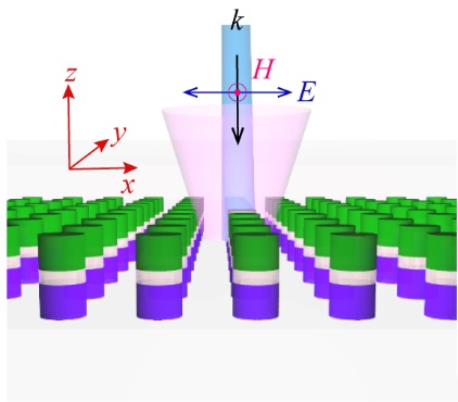
 Representative image of 2D array of PT symmetric nanoantennas (See reference [2] for details)
A major challenge in plasmonics, which has been actively studied for over a decade, is the large optical loss which degrades the performance of most plasmonic devices. High index dielectric materials provide a promising alternative route to realize many of the functionalities achievable in plasmonics. Distinctive advantages of high index dielectric resonant nanostructures over their metallic counterparts are low dissipative losses and the existence of both electric and magnetic resonances of comparable strengths. Moreover, semiconductor nanostructures like III-V materials with optical gain provide a route to design active nanophotonic devices. In our research we investigate methods to improve optical gain in nanostructures. We are interested in design and implementation of high Q cavities for light emission from Semiconductor Nanostructures. We also aim to seek a judicious engineering of the interplay between gain, loss and coupling in (parity-time) PT-symmetric nanostructures in order to design directional light-emitting devices with non-trivial characteristics. Some of our recent work is highlighted below:
Investigation of the carrier surface recombination in III-V semiconductors for on-chip nanophotonic applications
Our numerical investigation of carrier dynamics in GaAs nanocylinder on optical pumping lead us to estimate the qualitative and quantitative impact of surface recombination on the optical gain. The optically induced carrier density is lower in nanocylinder due to the dangling bonds at the surface that give rise to recombination of electron hole pairs. With reduced dimensions of the nanostructures, surface area-to-volume (A/V) ratio increases, and therefore the lasing threshold also increases due to higher non-radiative surface recombination process. The optical gain and bandwidth both reduce with increasing surface recombination velocity (SRV). The study gives an insight that p-doping of active material and strain incorporation as a viable approach for enhancing luminescence quantum yield of III-V semiconductor nanostructures. This can complements the surface passivation techniques widely adopted in the III-V research community.

Figure 1: Impact of Surface Recombination and nanocylinder size on optical gain. Further details can be found in reference [1]
PT-symmetric semiconductor nanoantenna metasurface
The concept of (parity-time) PT symmetry has opened a fundamentally new chapter in photonics and expanded the toolbox of photonics by broadening the design parameter space. In the context of photonics, PT symmetry can be realized by requiring an even distribution in the real part of the refractive index, and an antisymmetric gain/loss profile, associated with the imaginary part of the refractive index. The interplay of gain-loss contrast and coupling in PT-symmetric systems has manifested as a number of intriguing breakthrough effects like single-mode lasing, unidirectional invisibility, (coherent perfect absorber) CPA-laser, etc. In this project, we investigated vertically stacked GaInP PT-symmetric nanodisk resonators arranged in two-dimensional periodic lattice using full-wave numerical simulations and scattering matrix theory. The proposed dielectric metasurface supports spectral singularities (SS) with asymmetric reflection and highly anisotropic far-field scattering patterns. At SS, the scattering coefficients tend to infinity, corresponding to lasing threshold. This lasing spectral singularities can occur only in the presence of gain and being poles of the scattering matrix at real frequencies, imply zero-width resonances. Our analysis suggests that a proper combination of geometry, gain, and subwavelength resonances provides flexibility for designing tunable and directional nanophotonic light sources employing non-Hermitian physics.

Figure 2: PT symmetric nanostructures can be designed to exhibit extremely narrow-width resonances known as Spectral Singularities. Further details can be found in reference [2].
Jinal presented her research at the prestegious Frontiers in Optics conference held virtually in September 2020. Hope you will find the video of her talk informative.
References
- Jinal Kiran Tapar, Saurabh Kishen, Kumar Prashant, Kaushik Nayak and Naresh Kumar Emani. Enhancement of the optical gain in GaAs nanocylinders for nanophotonic applications. Journal of Applied Physics, 127, 153102 (2020). [ doi | pdf ]
- Jinal Kiran Tapar, Saurabh Kishen and Naresh Kumar Emani. Spectral singularities and asymmetric light scattering in PT-symmetric 2D nanoantenna arrays. Optics Letters, 45, 18, pp. 5185-5188 (2020). [ doi ]